

29 December 2006
 Prof. John Rogers at the University of Illinois, Urbana-Champaign, and his coworkers have developed a printing technique that allows them to combine a wide variety of inorganic structures, such as single-walled carbon nanotubes, assorted nanoscale wires, and ribbons made of gallium arsenide or silicon, to create multilayered, high-performance optical and electronic devices. They can also print on flexible or curved surfaces.
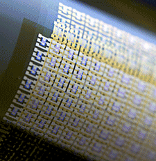
Rogers's method begins with the fabrication of nano- and microstructures, such as an array of semiconducting silicon nanowires, using conventional techniques. The researchers then press a soft stamp onto these structures, and when the stamp is peeled away, the structures stick to it, much as dust will cling to a strip of tape. The nanostructure-bearing stamp is then pressed onto another surface that is covered with a glue-like polymer. Once this polymer cures, it adheres to the nanostructures more strongly than to the stamp: when the stamp is lifted off, it leaves the nanostructures behind, still ordered in the same configuration in which they were originally patterned. This is then repeated for the other structures.
The research has been published in the Dec. 15, 2006 issue of Science.
(via TechnologyReview, Image Credit: John Rogers)
0 Comments:


All Topics
Etc