

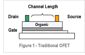
 As shown in Figure 1, conventional design of OFETs has a lateral structure. The space between the source and the drain needs to be minimized in order to reduce voltage need and to increase current output of the OFETs. However, such a requirement is often limited by the fabrication techniques. Moreover, conventional design requires the gate to be located between the source and the drain, which limits the cross-sectional area for current flow and therefore limiting current output.
The above limitations of conventional OFETs might be overcome by a novel design, the vertical organic field effect transistor (VOFET). Invented by the Yang Yang Laboratory at UCLA, and licensed to ORFID Corp., VOFET has a vertical structure, where gate-source-drain are arranged layer-by-layer (Fig. 2).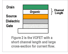 The device consists of two major cells. The first is an active cell (drain/organic/source) vertically stacked on top of a capacitor cell (source/dielectric/gate). These two cells share (are joined by) a common-source electrode.
This unique design allows a very short channel length (less than 0.1 µm) between the source and drain and an extremely large cross-sectional area, allowing low operating voltages (less than 5 V) and high current outputs (up to 10 mA). Also, such layered VOFETs are suitable for low-cost fabrication techniques, such as roll-to-roll printing.
See the following video for demonstration:
(Image and video source: www.orfid.com)


